Similar Posts
Role of Entrance Mosfet Layer in DC to DC Converters
14 Aug 2023
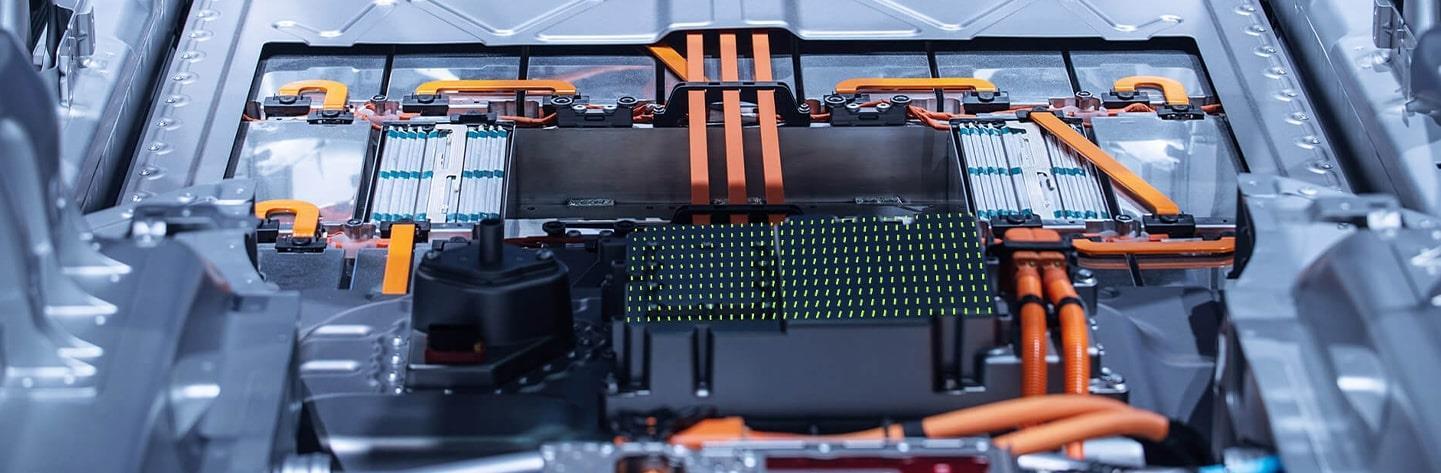
DC to DC converters are pivotal in modern electronics, ensuring efficient power management in devices ranging from mobile phones to electric vehicles. At the heart of these converters lies a critical component: the Entrance Mosfet Layer. This blog post delves into its role and why it's revolutionizing power conversion efficiency.
Basics of DC to DC Converters
DC to DC converters are electronic circuits used to convert a source of direct current (DC) from one voltage level to another. They are essential in applications where the voltage provided by power sources needs to be adjusted to match the requirements of electrical devices. Common types include Buck converters (step-down), Boost converters (step-up), and Buck-Boost converters (variable step-up/step-down). Key components include inductors, capacitors, diodes, and, importantly, MOSFETs, which regulate power flow.
Introduction to Entrance Mosfet Layer
The Entrance Mosfet Layer is a specialized type of MOSFET designed specifically for DC to DC converters. It offers improved performance compared to traditional MOSFETs, thanks to its unique structure that minimizes resistance and maximizes current flow. This layer plays a crucial role in the efficient conversion of power within these systems.
Benefits of Using Entrance Mosfet Layer
Incorporating the Entrance Mosfet Layer in converters leads to several benefits:
- Improved Efficiency: It reduces energy loss during conversion, leading to more efficient power use.
- Reduced Heat Dissipation: Less energy loss means lower heat generation, enhancing the durability of the device.
- Enhanced Power Handling: It can handle higher currents, allowing for smaller and more powerful converters.
- Compact Design: Its efficiency allows for smaller component sizes, reducing the overall size and weight of the converter.
Technical Deep Dive into Entrance Mosfet Layer
The Entrance Mosfet Layer operates by reducing the resistance encountered during the conversion process. This is achieved through advanced semiconductor materials and innovative design that optimize electron flow. Case studies in high-performance computing and renewable energy systems illustrate its effectiveness in diverse applications.
Future Prospects
The future looks bright for the Entrance Mosfet Layer with ongoing research aimed at further reducing costs and enhancing compatibility. Advancements in semiconductor technology hold promise for even greater efficiency and miniaturization in DC to DC converters.
Conclusion
The Entrance Mosfet Layer is a game-changer in the world of power conversion. Its ability to enhance efficiency and reduce size in DC to DC converters is key in an era where power demands are constantly increasing. As technology progresses, its role is set to become even more pivotal.
Similar Posts
References
Our Partners